|
January 2019
AutomatedBuildings.com
|
[an error occurred while processing this directive]
(Click
Message to Learn More)
|
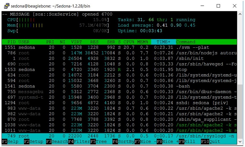
The Processor
Above
we have the Sedona
framework running on the Octavo OSD3358-512M-BSM.
The Octavo chip is known as a System in Package or (SiP) houses a Texas
Instruments AM3358
processor at 1GHz as well as 512Mb of RAM and full
power management system, all integrated into a single device. In this
small test, we have a 100-component Sedona DDC app and a single SOX
connection. The app execution rate is set to ten milliseconds. This
means that the DDC app will be scanned through 100 times every second,
(Running the app at this frequency is somewhat of an extreme use case).
At the end of every app cycle, the Sedona Virtual Machine (SVM) also
processes any outstanding work required by all service components that
are running on the platform (such as the SOX session). It does all of
this from within the context of the SVM executable. After each engine
scan, the app and SVM will go to sleep until the next scheduled scan
cycle.
That
last paragraph was an earful... Sorry. But it’s necessary to frame
the topic we are about to discuss today; the Edge Processor.
As you can
see from this example above, the single Cortex-A8
core listed as “CPU”
in the upper left corner is running at about 15.0 percent of its
capacity. Of that total processing time, the “SVM process” which is
listed as PID 1551 is consuming 20.7 percent of the core’s total
computing efforts. The rest of the CPU’s time is committed to doing
other things.
Those
other things are all listed there as well. They each have a
unique “PID” or Process IDentification. Every individual running
process consists of one or more threads. A thread is a fundamental unit
of code execution. It’s the path the CPU takes as it navigates through
a particular piece of software; whether that involves completing a
series of consecutive instructions, looping through the same code
several times, or following some kind of fork in the road to another
set of functions. We can see that there are currently 66 threads
executing on our processor at this moment. It was mentioned before that
the Sedona app executes and then goes to sleep. This is an example of a
thread running and then blocking. Blocking means that the
thread runs,
and then pauses while it waits for some other event to occur. In this
case, the event is the time until the next engine scan. Hopefully, our
SVM got everything done in that 10-millisecond window and will go to
sleep for the remaining period until it’s time to run again for the
next cycle.
One
important thing to know is that our CPU does not run this thread
continuously until it blocks. In reality, it’s actually rapidly
changing between all 66 threads, as long as they are also not blocked.
It runs a little bit of code from one thread and then rapidly switches
context to run code for another. This is the nature of an applications
processor. These devices, which almost always use operating
systems,
switch rapidly between threads giving the illusion that many things are
all happening at once. Processors that are designed to support
operating systems with this kind of preemptive multitasking
capability
are what make a device an Edge Controller.
Contrast
our CPU here to the action of a microcontroller.
Microcontrollers are simpler processing devices with much less
complicated hardware. The internal architecture is designed such that
these devices would normally run a single thread only. In other words,
they were designed to do only one thing. Sedona was designed to execute
as a single thread exactly for this reason; so that it could be used on
a low-cost microcontroller. At that time, that was all that was
realistically available from a hardware cost perspective. This is no
longer true today. Applications processors are now widely available and
also inexpensive. So, if the microcontroller was good enough for what
we were doing before, why would we move to use components that are much
more complex? Why are all the major manufacturers of controls adopting
these applications processors in their new devices? The answer is that
these days we need our field devices to do more. The reason for this is
the same reason all new smart devices use this type of hardware:
- Increased bandwidth to support secure encrypted communications.
- The ability to handle multiple applications, services, and
connections at once.
- Maintainability; the ability to apply firmware and security
updates.
A
programmable field controller has to be much more than it has been in
the past: a flexible, secure, data-crunching, sensor hub that connects
to anywhere in the world, rather than a slow, esoteric, plastic box,
that mindlessly churns through the same setpoint code every day. So
then, if the microcontroller cannot do all these things, is it dead for
use in controls? Not at all.
[an error occurred while processing this directive]
The
virtues of the microcontroller are:
- Lower power.
- Deterministic code execution.
- Fast booting and extremely reliable.
Consider
for example the case of a smart Electric Meter. We all know AC
current takes the form of a sinusoidal wave. Here in North America,
that waveform is of course 60Hz. To capture information about
electrical usage, we must continuously capture sensor samples at
regular intervals. Per the Nyquist theorem, we must sample this wave at
a minimum of at least 120Hz. In fact, we must sample at an even greater
frequency to have any chance to be accurate. Comparing this requirement
to our Sedona engine scan example from above, the 100Hz SVM scan
frequency, even though extreme for the Sedona world, isn’t even close
to what is needed. We would have to move this particular sampling task
to a completely different processing context. Not only that, but the
main CPU core we are using is not even appropriate for this job.
The
Cortex-A8 application core is designed for high throughput and not
determinism. That is to say, it can do a lot at once, but cannot
guarantee when any of it gets done. Our edge processor cannot fail to
take a sample at the correct time interval, or else all sensor accuracy
will be lost. For that matter, it also can’t miss that SVM engine scan
every 10ms. Care must be taken to give the Sedona process the highest
priority in the thread scheduler. The real-time sampling use case is an
area where the microcontroller core dominates. Because its hardware is
simpler, it’s better at doing just one thing predictably, and reliably,
and at regular intervals. It would be best to offload these kinds of
tasks to microcontrollers and leave the less time-critical tasks to the
apps processor.
Or
even better, what if both processing cores could somehow be tethered
to together on a single device and share certain resources? The
application core would run the main OS and is responsible for PC or
server-like duties, while the microcontroller core(s) are independently
dedicated to single real-time measurement and control processes.
Fortunately for us, this has already been thought of. This particular
chip, as well as many others, have multiple cores! The AM3358 is
actually a multi-core device. It has a single ARM core, a graphics
processor, plus two microcontroller cores known as Programmable
Real-time Units (PRU). These additional microcontrollers were
included
specifically for performing real-time processing independently from the
main CPU core. This is very different than a desktop PC having multiple
cores. Personal computers have multiple cores to distribute the
workload for the same types of tasks. Embedded Edge Processors have
multiple cores to specialize in specific tasks. This is known as
Heterogenous System Architecture.
This
high level of silicon integration is what is fueling the
revolution of digital controls. Much of the groundwork has been laid
out by the SOC developers as well as the software engineers
who have
ported their operating systems to these devices. Consider this recent
announcement from the Linux Foundation regarding support for
open-source RISC-V processor cores. The infrastructure
supporting these
tiny devices has been created and is being continuously supported. It
took a tremendous effort by many to pack so much value into a single
silicon wafer.
Whatever
cannot fit on the applications processor die itself, such as
RAM and flash memory is being packaged into ever-shrinking modules,
such as our OSD3358 above. Devices such as these take advantage of
recent advancements in packaging technology, in addition to all of the
silicon integration we have seen. This tiny, postage-stamp-size chip is
a fully integrated processing system. Which is another way of saying
it’s a full PC on a single chip. The only thing its lacking is a
screen, keyboard, and mouse. If you needed to add one, you could.
Instead, we will be gluing this device to an Edge Controller baseboard.
Hope to see you next month when we will talk about that topic in The
Hardware.
footer
[an error occurred while processing this directive]
[Click Banner To Learn More]
[Home Page] [The
Automator] [About] [Subscribe
] [Contact
Us]